
In the rapidly evolving world of electronics manufacturing, choosing the right method for producing components is crucial. Metal stamping stands out as a preferred choice for many, but why? Let’s explore the reasons behind its popularity.
Metal stamping is favored for electronic components because it has a fast processing time and requires less labor than other methods.
To fully grasp the advantages of metal stamping in electronics, let’s delve deeper into its benefits and applications.
The Rise of Metal Stamping in Electronics
As the electronics industry has evolved, so too have the methods used to produce its components. Among these, metal stamping has emerged as a dominant force, offering unparalleled advantages in both efficiency and precision.
A Brief History
The journey of metal stamping in electronics can be traced back to the mid-20th century. As the demand for electronic goods surged post World War II, manufacturers sought faster, more efficient ways to produce components. Enter metal stamping. Initially adopted for its speed and cost-effectiveness, it quickly became evident that stamping also offered exceptional precision—critical for the intricate components of electronic devices. Over the decades, as technology advanced, metal stamping adapted, incorporating newer techniques and materials, ensuring its position as an indispensable tool in the electronics manufacturing arsenal.
Key Applications
Metal stamping’s versatility is evident in the wide array of electronic components it helps produce. Some of the primary applications include:
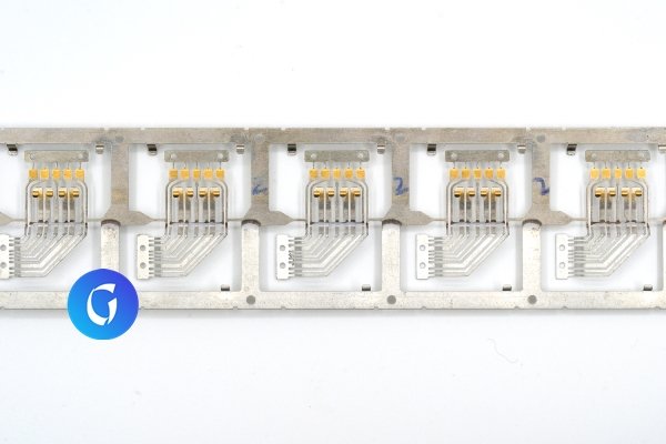
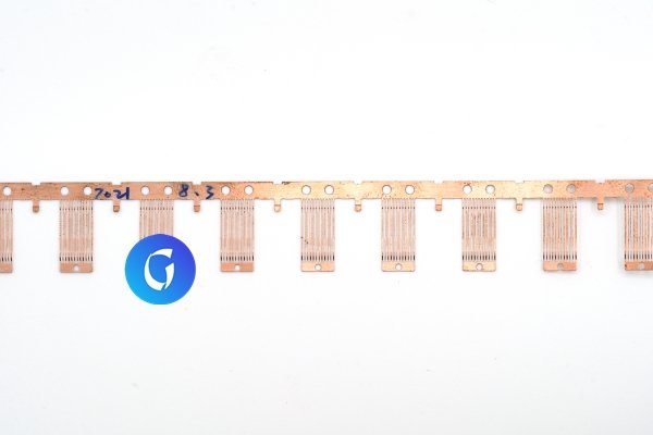
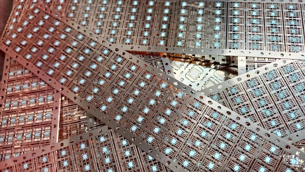
- Connectors: These tiny components, responsible for connecting different parts of an electronic device, are often produced using precision stamping to ensure a perfect fit and reliable performance.
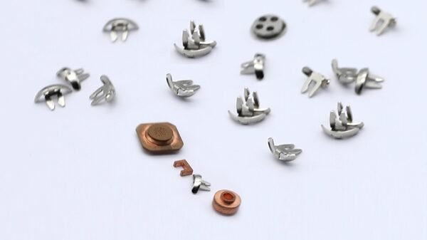
- Shields: Metal stamping is used to create electromagnetic shields that protect sensitive electronic components from interference.
- Terminals: These are the end points of electrical connections, and their precision is crucial. Stamping ensures they are consistent and of high quality.
- Lead Frames: Used in semiconductor packaging, these are produced with intricate designs, made possible through advanced stamping techniques.
- Heat Sinks: Essential for dissipating heat in electronic devices, these are often stamped from metals with high thermal conductivity.
From everyday gadgets to advanced aerospace equipment, metal stamping plays a pivotal role in shaping the electronics we rely on daily.
Advantages of Metal Stamping for Electronic Components
In the intricate world of electronics manufacturing, precision, speed, and cost-effectiveness are paramount. Metal stamping, with its unique attributes, has proven to be an invaluable asset in this domain. Let’s delve into the specific advantages it brings to the table.
Speed and Efficiency
In an industry where time is often equated with money, the swift processing capability of metal stamping is a game-changer. Traditional methods might require multiple steps and processes, but stamping can achieve the desired shape or form in a single press. This rapid production rate is especially beneficial in the electronics sector, where market demands can fluctuate, and manufacturers need to adapt quickly. With metal stamping, large batches of components can be produced in a fraction of the time, ensuring that supply always meets demand.
Labor Efficiency
Beyond the sheer speed of production, metal stamping also offers significant labor efficiencies. Automated stamping presses can operate with minimal human intervention, reducing the need for extensive manual labor. This not only translates to cost savings but also ensures a consistent production quality, free from human error. In an industry where precision is non-negotiable, this level of reliability is invaluable.
Precision and Consistency
Speaking of precision, metal stamping excels in producing components with exacting standards. The dies used in stamping are crafted with meticulous attention to detail, ensuring that every component produced is consistent with the last. In the realm of electronics, where even the slightest deviation can lead to functional discrepancies, this consistency is crucial. Whether it’s connectors that need to fit just right or shields that must offer precise protection, metal stamping ensures that every part is up to the mark, every single time.
Comparing Metal Stamping to Other Methods
While metal stamping has carved a niche for itself in the electronics industry, it’s essential to understand how it stacks up against other manufacturing methods. Let’s delve into a comparative analysis.
Metal Stamping vs. Casting
Both metal stamping and casting are popular methods for shaping metal, but they serve different purposes and have distinct characteristics:
- Process: Metal stamping involves shaping flat metal sheets using dies and presses. In contrast, casting requires melting the metal and pouring it into molds where it solidifies into the desired shape.
- Precision: Stamping is known for its high precision, especially for thin and flat components. Casting, while versatile in creating complex shapes, might not achieve the same level of precision for certain electronic components.
- Material Waste: Stamping produces minimal waste as it shapes the metal directly into the desired form. Casting, on the other hand, might result in more material wastage, especially if the cast requires further machining or finishing.
- Applications in Electronics: Stamping is often preferred for components like connectors, terminals, and shields. Casting might be more suitable for larger, bulkier parts or when a specific metal alloy is required.
Cost Implications
When it comes to cost, several factors come into play:
- Initial Setup: Metal stamping requires an investment in designing and creating dies, which can be expensive. However, once set up, the cost per component is relatively low. Casting molds can also be costly, but the recurring costs might vary based on the complexity of the component and the type of casting method used.
- Labor Costs: As mentioned earlier, metal stamping, especially when automated, can significantly reduce labor costs. Casting, depending on the method (e.g., die casting vs. sand casting), might require more manual intervention and thus higher labor costs.
- Material Costs: Stamping usually results in less material wastage, leading to cost savings. Casting might require more raw material, especially if there’s a need for post-casting processes.
- Volume: For large production runs, the per-unit cost of stamped components often becomes more economical. Casting might be more cost-effective for smaller batches or specialized components.
Real-world Applications and Case Studies
Metal stamping’s prominence in the electronics industry isn’t just theoretical. Numerous companies have reaped tangible benefits from its application, and continuous innovations ensure its relevance in the ever-evolving tech landscape.
Success Stories
- TechGiant Inc.: A leading electronics manufacturer, TechGiant Inc., transitioned from traditional machining to metal stamping for their line of connectors. The result? A 30% reduction in production costs and a 25% increase in production speed, allowing them to meet the surging market demand efficiently.
- ElectroWave Solutions: Specializing in wireless communication devices, ElectroWave Solutions adopted metal stamping for producing electromagnetic shields. The precision offered by stamping ensured optimal device performance, leading to a 15% increase in customer satisfaction ratings.
- NanoTech Components: In the realm of microelectronics, NanoTech Components leveraged the precision of metal stamping to produce ultra-thin terminals for their next-gen chips. The outcome was a product line that was not only more reliable but also more competitive in the market.
Innovations in Stamping
The world of metal stamping isn’t static. As the demands of the electronics industry evolve, so do the techniques and technologies in stamping:
- High-Speed Stamping: Recent advancements have led to the development of high-speed stamping presses that can produce components at unprecedented speeds, catering to industries where time-to-market is critical.
- Precision Micro-stamping: With the miniaturization trend in electronics, there’s a growing need for micro-components. Precision micro-stamping techniques now allow for the production of parts as thin as a few micrometers with impeccable accuracy.
- Hybrid Stamping: Combining traditional stamping with other processes like forging has given birth to hybrid stamping. This method harnesses the best of both worlds, allowing for the creation of components with enhanced structural integrity without compromising on precision.
- Smart Dies: The integration of sensors and AI in stamping dies enables real-time monitoring of the stamping process. This not only ensures consistent quality but also predicts die wear, reducing downtimes and ensuring uninterrupted production.

Conclusion
Metal stamping, with its blend of speed, precision, and cost-effectiveness, has firmly established itself as a cornerstone in the electronics manufacturing landscape. From the intricate connectors that power our favorite gadgets to the electromagnetic shields ensuring optimal device performance, stamping plays a pivotal role in bringing technology to life.
Its advantages are not just theoretical. As showcased through real-world success stories, companies across the spectrum have harnessed the power of stamping to drive efficiency, reduce costs, and enhance product quality. And with continuous innovations, from high-speed presses to smart dies, the future of metal stamping in electronics looks brighter than ever.
In an industry marked by relentless evolution and rising consumer expectations, metal stamping offers a robust solution to meet these challenges head-on. For manufacturers aiming to stay ahead of the curve, embracing the myriad benefits of metal stamping isn’t just a strategic choice—it’s an imperative for sustained success in the dynamic world of electronics.


2 Responses
I was captivated when you mentioned that our life largely relies on electronic products. My friend needs electrical components. I should advise him to look for a reliable YuCo replacement ABB EH contactor.
thanks for share, helpful.